How To Make Test Points In Altium
Altium nets Identifying minimum pcb trace spacing and width in altium designer Altium 3d components designer
Altium PCB Designer: Test Point Manager Design Rules
Altium testpoint riege modified Altium pcb designer: test point manager design rules How to use pcb testpoints
How to make 3d components in altium designer
Altium designer tips #2: how to use test point managerIdentifying minimum pcb trace spacing and width in altium designer Altium define separate constrain vias rulesAltium scope.
Altium productivity designer features point test advantage take violations notifications clearance instant adWhat is a test point pcb? New productivity features to take advantage of in altium designer 15.1Adding snap points to a 3d model in altium designer.

Is it printed or a component? all about pcb test points
How to create a test point schematic symbol and footprint in altiumAdding test-points Altium test point designerAltium pcb manager testpoint use menu designer test points point.
Test points in altium schematicTest point altium symbol schematic create footprint designer testing created updated november april Circuit board design for in-circuit testingIdentifying minimum pcb trace spacing and circuit board requirements in.

Altium pcb designer test use menu rules point points
Adding testpoints to a pcb in altium designerAdding testpoints to the board Altium tutorialAltium tab track.
How to create a test point schematic symbol and footprint in altiumSchematic test point symbol altium create designer footprint How to use pcb testpointsAltium pcb manager use testpoint menu designer test points now successfully assigned point.

How to use pcb testpoints
Adding testpoints to a pcb in altium designerAltium designer testpoint pcb test points use menu setting styles Altium pcb designer: test point manager design rulesAltium trace minimum spacing identifying requirements values rule routing width pcb constraint changing.
Altium designer pcb use test points point usages settingAdding testpoints to a pcb in altium designer Altium documentation testpoint outputs versatile configuration configure contained fabrication output include assembly within once job self report fileHow to use pcb testpoints.

Adding testpoints to a pcb in altium designer
Altium pcb designer test points use thru testpoint manually setting holeAdding testpoints to the board Testpoint setupStraighten schematic connections in altium.
How to use pcb testpointsIdentifying minimum pcb trace spacing and width in altium designer How to use pcb testpoints.


Adding Testpoints to a PCB in Altium Designer | Altium Designer 22 User

How to Use PCB Testpoints | Altium Designer

Adding Testpoints to a PCB in Altium Designer | Altium Designer 22 User

Identifying Minimum PCB Trace Spacing and Width in Altium Designer | Altium
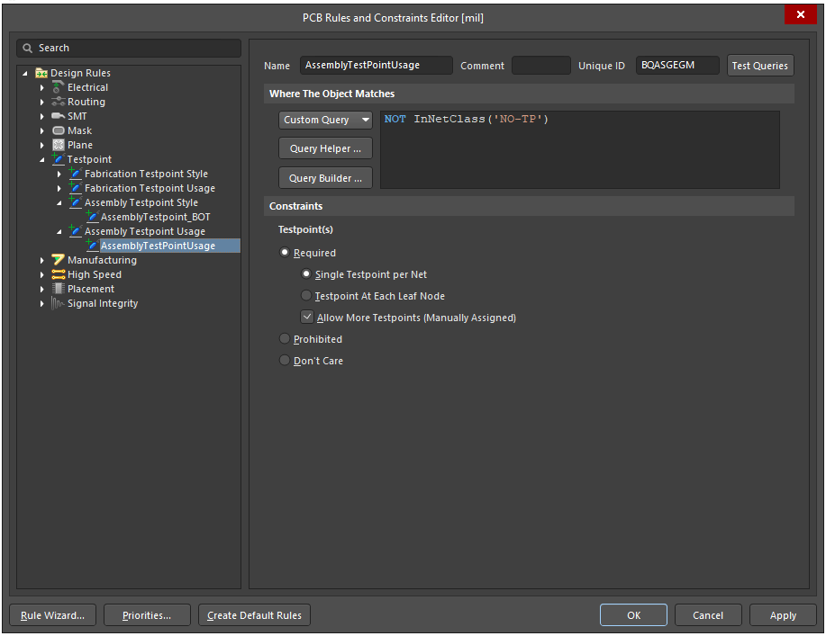
Altium PCB Designer: Test Point Manager Design Rules

What is a Test Point PCB? - RAYPCB

Testpoint Setup | Altium Designer 19.0 Technical Documentation