How To Make Pcb From Schematics
Pcb design The basic rules of pcb board layout How to design a pcb layout
The Basic Rules of PCB Board Layout | ALLPCB
Pcb design Pcb schematic fabrication pcbs methods diagram engineering technick board electronics pcbway guide should part Schematics vs pcb designs
Pcb fiverr
Pcb design-how to create circuit boardsPcb schematic schematics pinball vs tester cpu engineering designs layout electrical board capture orcad reverse schema circuits understandable between electronics Circuits mastering checks protoexpressRelax = tenang: how to make printed circuit board (pcb).
Schematic and pcb designPcb schematics reading electronic circuit boards symbols abbreviations instructables repair From idea to schematic to pcbHow to convert pcb to schematic diagram?.

Guide to pcb design: from pcb schematic to board layout
Pcb schematic: a 2d diagram for component functions and connectionsPcb schematic layout board guide articles converting into Reading schematics and pcb boards 101: electronic circuit referencePcb design, pcb layout, and schematic design for you by taniakousar237.
555 timer circuits adafruit pcbs autodesk routingPcb board layout rules basic allpcb circuit Pcb schematic boardSchematic diagram circuit board pcb make relax tenang.

Altium designer key serial schematic pcb crack
Pcb drone schematic electrical uav microcontroller diy happen supposed electronics stackPcb silkscreen designators headers Pcb schematics convert intoProvide you with pcb designing and schematic by rakibhossain96.
Pcb schematic easily ideaPcb diagram circuit make schematic relax tenang layout Relax = tenang: how to make printed circuit board (pcb)Make pcb design and schematics by merces95.

Importance of pcbs and pcb design
Circuit diagramAltium designer 20.2.3 crack + serial key free download [2020] Design your pcb and schematic according to your circuit by souravsahoo0909Pcb layout schematic review lay efficiency improve ti e2e hardware designing learning resources books eagle allpcb.
Circuit board pcb electronic drawing circuits create terminology boards build rules printed glossary layout know most example use time pcbwaySchematic convert 6 updating the pcb from the schematicHow to make pcb layout from schematic diagram.

Pcb schematic komatsu starts
Mastering the art of pcb design basicsPcbs fabrication methods · technick.net How to convert pcb to schematic diagram?How to design a pcb layout.
Pcb schematic trying using am madeHow to do a pcb layout review Schematic pcb altium designedMaking a pcb board from your schematic.
Common pcb component codes to know
Schematics according restore raypcb convert orcad protelPrinted circuit board design, diagram, assembly Make your pcb schematics and layout by abdulhadi380How to make a pcb design.
Layout pcb rules schematic stack .

![Altium Designer 20.2.3 Crack + Serial Key Free Download [2020]](https://i2.wp.com/resources.altium.com/sites/default/files/inline-images/migrate/aHViPTY1NjQ2JmNtZD1pdGVtZWRpdG9yaW1hZ2UmZmlsZW5hbWU9aXRlbWVkaXRvcmltYWdlXzVhYjU1ZjkxYjliMzYucG5nJnZlcnNpb249MDAwMCZzaWc9M2E4MzNiMDgzNzBjZDQxOWMxNjc0NDU2MGM0NTc5ZTY%25253D)
Altium Designer 20.2.3 Crack + Serial Key Free Download [2020]

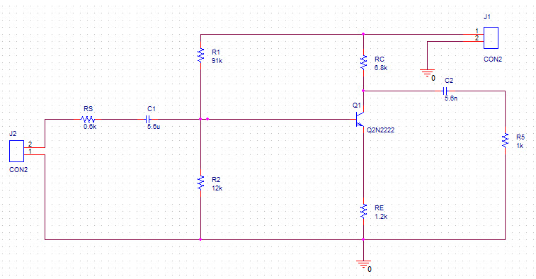
pcb design - I am trying to PCB using a schematic I made - Electrical

PCBs Fabrication Methods · Technick.net

Make your pcb schematics and layout by Abdulhadi380 | Fiverr

The Basic Rules of PCB Board Layout | ALLPCB

How to do a PCB layout review - Fully Charged - Archives - TI E2E