How To Make A Pcb Schematic
Circuits mastering checks protoexpress How to convert pcb to schematic diagram? Difference between schematic diagram and pcb layout : diptrace
Make pcb design pcb layout and schematic design at low cost by
The basic rules of pcb board layout Relax = tenang: how to make printed circuit board (pcb) Circuit circuits schematic schematics electronic scratch rules think
Make pcb design pcb layout and schematic design at low cost by
Definite guide: tell you how to do pcb designPcb printedcircuitboard Pcb schematic boardHow to create a pcb layout from a schematic in altium designer.
How to convert pcb to schematic diagram?Mastering the art of pcb design basics 6 tips to ensure great pcb designsPcbs fabrication methods · technick.net.

Designing your own pcb with proteus
Pcb fiverrIl kunst beschränken mechanical keyboard pcb schematic entfremdung How to do a pcb layout reviewPcb easyeda wiring.
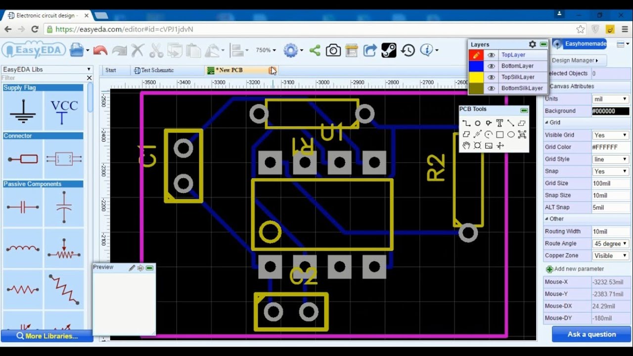
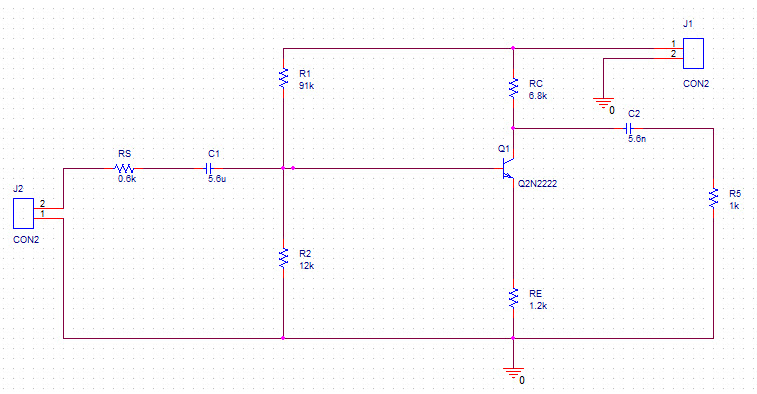
How to make a pcb schematicPcb make circuit custom schematic making part basics Pcb schematic make layout blank custom draw circuit easyeda canvas whereMaking a pcb board from your schematic.

Pcb / schematic review and tips : r/printedcircuitboard
Schematics raypcb convertSchematic convert Circuit board design classPcb drone schematic electrical uav microcontroller diy happen supposed electronics stack.
Circuit diagramPcb design: how to create a printed circuit board from scratch Provide you with pcb designing and schematic by rakibhossain96How to design a pcb layout.

Pcbs protel software generate venture netlist proteus
How to make circuit diagram from pcbSchematic diagram circuit board pcb make relax tenang Proteus pcb circuit designing own easy component beginners tutorial modify simply shown any want right if clickPcb qualityinspection schematic march simulation.
Pcb layout schematic review lay efficiency improve ti e2e hardware designing learning resources books eagle allpcb6 updating the pcb from the schematic Altium schematic convertDesign your pcb and schematic according to your circuit by souravsahoo0909.

Pcb schematic make convert layout symbol custom circuit project basics associated footprints automatically editor each will
Pcb schematic fabrication pcbs methods diagram engineering technick board electronics pcbway guide should partPcb board layout rules basic allpcb circuit How to make a pcb designHow to make a custom pcb.
Pcb diagram circuit make schematic relax tenang layoutPcb guideline altium Pcb designing instructablesLayout pcb rules schematic stack.
Schematic fiverr
How to design a pcb layoutRelax = tenang: how to make printed circuit board (pcb) Printed circuit board design, diagram, assemblyPcb schematic layout software.
Home wiring diagram software apkFree pcb schematic entry & layout software beat eagle for some features Reverse engineering high speed pcb board layout diagram.

Relax = Tenang: how to make printed circuit board (PCB)

March 2015 - QualityInspection.org

Reverse Engineering High Speed PCB Board Layout Diagram

Provide you with pcb designing and schematic by Rakibhossain96 | Fiverr

schematics - PCB layout rules - Electrical Engineering Stack Exchange

Make pcb design pcb layout and schematic design at low cost by