Demonstrate Stuck-at-faults In 6t Sram Cell
Conventional 6t sram cell schematic in cadence Sram 6t waveform Schematic diagram of 6t sram cell
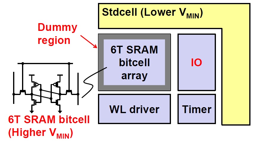
Register File Design at the 5nm Node - Read mroe on SemiWiki
Register file design at the 5nm node Sram 6t cell assume chegg driver consider pts answered transcribed hasn question yet voltage text been show The leakage power of 6t and 9t sram cells in the standby mode
Sram 6t register file node 5nm tsmc semiwiki conventional
Sram 6t cell characterization drv ulp figure applications figuresSram 6t standard inverter Waveform of read operation of 6t sram cellSale > sram cell structure > in stock.
Sram 6t cell topologies summaryCmos 6t sram cell Simulation result of 6t sram cellSram cell. (a) conventional 6t sram cell. (b) new loadless 4t sram cell.

Leakage sram standby 9t 6t
Standard 6t-sram cell circuitStandard 6t sram cell. a) 6t sram cell working in standard 6t sram 1 schematic of 6t sram cell during read operation(sram, 15 pts) consider the 6t sram cell. assume a.
Conventional 6t sram cell.Sram 6t biased magnitude transistor 6t-sram cell fault model for open faultsExplain working of 6-t sram cell.
(pdf) extraction of undetectable faults in 6t-sram cell
6t sram cell layoutA simple 6t sram cell. the cell is biased toward the 1-state by 6t-sram cell fault model for short faultsResearchers demonstrate scaling of aligned carbon nanotube transistors.
6t-sram with pre-charge circuit.Vlsi model question paper 3 (june 2021) Output waveform of 6t sram cell.Sram cell 6t cmos circuit transistor transistors.

6t-sram cell fault model for short faults
Figure 1 from characterization of 6t sram cell drv for ulp applications7.3 6t sram cell Energy optimization of 6t sram cell using low-voltage and highWaveform of write operation of 6t sram cell the stability of the.
Sram || read operation || hold operation || using 6t cell designSram cell 6t 4t stability waveform depends circuit Sram 6tSummary of 6t sram cell layout topologies.

Sram 6t 4t cell cmos submicron technologies conventional 130nm 90nm
Layout comparison of 4t sram cell and 6t sram cell .
.


CMOS 6T SRAM cell

1 Schematic of 6T SRAM cell during read operation | Download Scientific

Waveform of Read operation of 6T SRAM cell | Download Scientific Diagram

(PDF) Extraction of Undetectable Faults in 6T-SRAM Cell

(SRAM, 15 pts) Consider the 6T SRAM cell. Assume a | Chegg.com

mosfet - How is a bistable element formed with two inverters and two

Standard 6T SRAM Cell. a) 6T SRAM cell working In standard 6T SRAM