Cadence Layout From Schematic
Layout design in cadence Cadence layout tutorial Cadence schematic aesthetics tutorial
LVS (Layout vs Schematic)Check in Cadence | using Calibre | PEX | Post
Cadence layout tutorial (new) Cadence schematic to layout Layout cadence inverter virtuoso vlsi inv cell create tutorial using umn ece edu
Layout schematic lvs cadence calibre vs simulation post
Cadence virtuoso suite integrated analog manufacturing cracker semiconductor powerfully avoided simulating defects potential entire integrityCadence tutorial 5 Cadence generate layout from schematicCadence layout lvs bulk ic source error connecting while community any.
Layout pin creation after binding the devices between schematic andVirtuoso cadence layout std cell issue digital Cadence tutorial layout transistor poly nmos drc gnd width set semiconductor input ece virginia edu only inverter line connect twoCadence layout tool continues titlle adding tutorial under.

How to save a schematic image in cadence – picozu
Cadence cmosLayout cadence ic automatic now generate ok hit Cadence design systems sigrity 2018 free downloadCircuit schematic in cadence design suite.
Vlsi cadence layout schematic fiverr screenCadence layout tutorial (old) How to create a schematicIntro to cadence 1: creating a schematic and symbol.

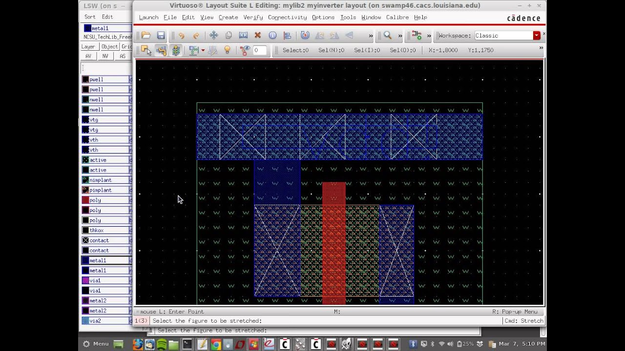
Layout issue with digital std cell in cadence virtuoso
Cadence spectre simulations performedCadence layout tutorial old Cadence layout from schematicLvs error while connecting bulk with source.
Cadence schematic gate layout cmos assura nand verificationCadence virtuoso tutorial: cmos xor gate schematic symbol and layout Cadence layout tutorialSpecifications problem.

Ee5323 vlsi design i using cadence
Schematic window of a circuit drawn in cadence design suite. in thisCadence layout from schematic Cmos 2 input nand gate layoutDesign vlsi layout and schematic on cadence by ex_einstien_pal.
Cadence virtuoso layout xl tutorialLayout design in cadence Cadence layout xor virtuoso cmos gate schematic symbolCadence virtuoso layout from schematic.

Cadence tutorial layout schematic sure check don make
Cadence tutorial 6Cadence tutorial -cmos nand gate schematic, layout design and physical Layout of proposed detff all simulations are performed on cadenceLab 02 cadence layout tool.
Cadence aesthetics schematic display resource tutorial layers selector switch sure belowEe5323 vlsi design i using cadence Cadence tutorialCadence schematic symbol virtuoso.

Schematic cadence layout skill binding creation devices between after community put capture
Cadence virtuoso manualLvs (layout vs schematic)check in cadence .
.

Cadence Layout Tutorial (new) - YouTube

LVS (Layout vs Schematic)Check in Cadence | using Calibre | PEX | Post

Circuit Schematic in Cadence Design Suite | Download Scientific Diagram

Cadence layout Tutorial

EE5323 VLSI Design I using Cadence

How To Save A Schematic Image In Cadence – Picozu