Altium Pcb Sheet Size
Layout guide to changing board sizes in altium designer How to design the perfect pcb stack up with altium designer What pcb copper thickness should you use?
Altium CircuitMaker – PaxSpace, Inc
Altium pcb Preparing the board for design transfer Altium designer pcb designer
Altium pcb design rules
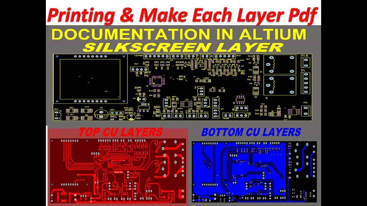
Pcb altium dimensions information opened thru reports menu which board stackPerfect styling for your organisation with altium 365 How to set the sheet size in altium designer?Altium circuitmaker – paxspace, inc.
Altium board changing sizes designer layout pcb setting originPcb board size altium Altium tutorial-21: how to print exact size layout layersAltium pcb component designer height thermal.

Altium sheet size designer set
Altium designer pcb design tutorialAltium pcb designer: get size from sheet layer Altium change pcb sizePcb altium tutorial designer string add click.
41 change pcb board size in altium designer 18Pcb design Pcb altium board wizard size values set define shape using another need way stackAltium designer reviews 2021: details, pricing, & features.

Altium pcb dimensions
Altium schematicAltium pcb Working with a design view object on a pcb in altium designerAltium designer pcb.
Altium pcbAltium pcb designer: get size from sheet layer Configuration & customization of altium designerAltium change pcb sheet size.

Altium outputs documentation sheet designer
Electronic – how to set the sheet size in altium designer – valuableAltium sheet mechanical contents preparing transfer board pcb print presentation linked been has More about outputsElectronic – how to set the sheet size in altium designer – valuable.
Pcb altium circuit maker circuitmaker eagle kicad geda software compete existing designspark block such kid cm tutorialAltium designer Altium sheet duplicate names netsLayout guide to changing board sizes in altium designer.

Set pcb size with values altium
Altium designer tutorialAltium properties select Altium board designer changing sizes cutout pcb addingSetting up a schematic document in altium designer.
Pcb designAltium board guide changing sizes layout designer Altium printLayer pcb altium mechanical assign.
Altium stackup stack
Pcb design using altium by sonu duhanLayout guide to changing board sizes in altium designer .
.


Working with a Design View Object on a PCB in Altium Designer | Altium

pcb - Component Height - Altium Designer - Electrical Engineering Stack

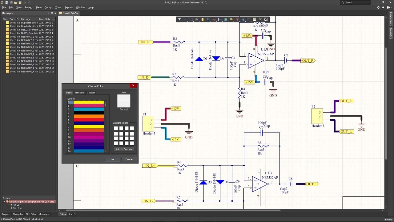
pcb design - Altium duplicate net names on top sheet - Electrical
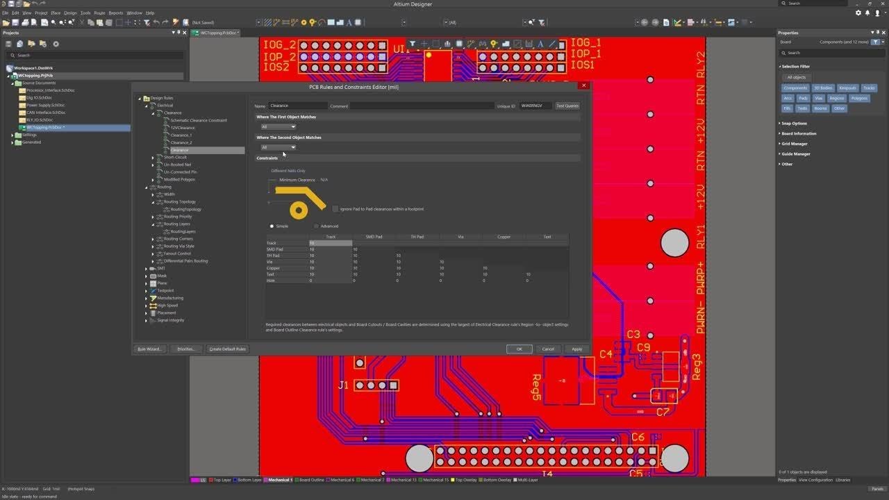
Altium pcb design rules - qlerobest
Altium schematic - garbay

Altium Designer PCB Design Tutorial | PCBCart